Pages

Pages

Wednesday, December 5, 2012

Mobile incoming call indicator


Description.
This circuit can be used to escape from the nuisance of mobile phone rings when you are at home. This circuit will give a visual indication if placed near a mobile phone even if the ringer is deactivated.
When a call is coming to the mobile phone, the transmitter inside it becomes activated. The  frequency of the transmitter is around 900MHz.The  coil L1 picks up these oscillations by induction and feds it to the base of Q1. This makes the transistor Q1 activated.Since the Collector of Q1 is connected to the pin 2 of IC1 (NE555) , the IC1 is triggered to make the LED connected at  its output pin (pin 3) to blink. The blinking of the LED is the indication of incoming call.

Circuit diagram with Parts list. 
Notes. 
  • The coil L1 can be made by making 150 turns of 36 SWG enameled copper wire on a 5mm dia plastic former.Or you can purchase a 10 uH coil from shop if available.
  • The circuit can be powered from a 6V battery.
  • Assemble the circuit on a good quality PCB.
  • C1 & C3 are to be polyester  capacitors.
  • The electrolytic capacitor C2 must be rated 10V.

Static 0 to 9 display

Description.
The circuit shown here is of a simple 0 to 9 display that can be employed in a lot of applications. The circuit is based on asynchronous decade counter 7490(IC2), a 7 segment display (D1), and a seven segment decoder/driver IC 7446 (IC1).
The seven segment display consists of 7 LEDs labelled ‘a’ through ‘g’. By forward biasing different LEDs, we can display the digits 0 through 9. Seven segment displays are of two types, common cathode and common anode. In common anode type anodes of all the seven LEDs are tied together, while in common cathode type all cathodes are tied together. The seven segment display used here is a common anode type .Resistor R1 to R7 are current limiting resistors. IC 7446 is a decoder/driver IC used to drive the seven segment display.
Working of this circuit is very simple. For every clock pulse the BCD output of the IC2 (7490) will advance by one bit. The IC1 (7446) will decode this BCD output to corresponding the seven segment form and will drive the display to indicate the corresponding digit.

Circuit diagram.


Notes.

§  The circuit can be assembled on a perf board.
§  Use 5V DC for powering the circuit.
§  The clock can be given to the pin 14 of IC2.
§  D1 must be a seven segment common anode display.
§  All ICs must be mounted on holders.

Saturday, November 24, 2012

UM66T MELODY IC

 The PCB contains just 2 components:


1. 10uF electrolytic capacitor
Make sure you insert this component with the positive lead (the long wire) facing right, with the strip on the body facing left. Push it most of the way into the PCB.

2. M66T IC
This has 3 wires. Spread the wires slightly and insert it with the flat
part of the case facing left. Push it about halfway into the PCB


CONNECTING THE SPEAKER


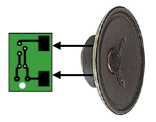
Now connect 2 solid core wires of about 30mm in length to the speaker terminals. Solder the other end to the large copper pads on the underside of the PCB.

POWER SUPPLY
 Left shows how to connect the battery, switch and PCB together.
You will need to either cut the positive lead, or add another wire to link the micro switch to the PCB. It depends how much wire you need.
Connect the power leads by feeding them up through the large hole first, then through the smaller holes.

Tuesday, November 13, 2012

TOUCH SWITCHS

TOUCH SWITCH 1

This circuit detects the skin resistance of a finger to deliver a awfully tiny current to the super-alpha try of transistors to show the circuit ON. The output of the "super transistor" activates the BC 557 transistor. The voltage on the highest of the world is passed to the front of the circuit via the 4M7 to require the place of your finger and also the circuit remains ON.

To turn the circuit OFF, a finger on the OFF pads can activate the primary transistor and this may rob the
"super transistor" of voltage and also the circuit can close up.

TOUCH SWITCH 2

This circuit detects the skin resistance of a finger to show the circuit ON for concerning one second. The output are often taken to a counting circuit. The circuit consumes no current when in quiescent mode:

Sunday, October 14, 2012

How to Transform a CD-ROM Drive into a Car CD Player


To be used as CD player, the CD-ROM drive doesn't need to be connected to the computer. This way, it is possible to easily transform a CD-ROM drive into a Car CD player. Sounds crazy? Not so. With this tutorial you will be able to have a CD player in your car without spending almost anything.

The CD-ROM drive to be use may be of any type, from the first models ("1x") until the most modern ones ("60x"). The only prerequisite is that the drive needs to have is an earphone plug and volume control. And practically all CD-ROM drives have that.

There are two great advantages in transforming a CD-ROM drive into a Car CD player. First, who will want to break your car window to take CD-ROM drive? And, secondly, since any type of CD-ROM drive can be used, you may take an old drive that is just dusting away in your house (for instance, a 2x drive from an old 386 computer), which brings the cost down to almost nothing.
To install a CD-ROM drive in the car, you will need a female power plug, to be used to fit into CD-ROM drive power plug (that plug can be cut from an old power supply) and a voltage regulating integrated circuit called 7805, that may be easily found at electronic parts stores. You will also have to buy a heat dissipator for the 7805 (sold at the same store).

The car battery is a 12 V one, but the CD-ROM drive needs two voltages to work: 12 V and 5 V. The 7805 circuit is able to convert a 12 V voltage into 5 V (its pin 1 is for the input, its pin 2 is the grounding, and its pin 3 is the 5 V exit). Figure 1 shows the plan for the connection. The grounding pin should be connected to the wires of the plug grounding and the negative pole of the car battery, what is done by simply connecting that pin to the metallic body of the car.


All you have to do is to make the connections shown in the above schematics (don't forget to isolate all connections with insulating tape) and you are set: you will have a CD-ROM drive working as CD player in your car.
 
The audio output will be made using the earphone plug. To listen to a CD, you will have to use earphones. To have the sound come through the speakers of the car, you will have to buy an amplifier with RCA inputs and a stereo P2 (mini jack) x stereo RCA cable (the same type of cable used to connect Discman units to amplifiers). The stereo P2 plug (also known as mini jack), which is the one used for the earphones, should be fit at the earphone output of the CD-ROM drive, while the RCA plugs should be fit at the input of the amplifier. The volume control will be made using the volume control in the CD-ROM drive.

A last warning: in most CD-ROM drives, the reproduction button (play) and the advance button (skip) are on the same key. In other words, to skip a track, all you have to do is to press the play button.


Monday, October 8, 2012

Digital Volume Control

This digital volume control has no pot to wear out and introduces almost no noise in the circuit. Instead, the volume is controlled by pressing UP and DOWN buttons. This simple circuit would be a great touch to any home audio project.


Parts:
Part
Total Qty.
Description
C1
1
0.1uf Ceramic Disc Capacitor
U1
1
DS1669 Digital Pot IC (See Notes)
S1, S2
2
Momentary Push Button Switch
MISC
1
Board, Wire, Socket For U1


Notes:
1. U1 is available from Dallas Semiconductor.
2. S1 turns the volume up, S2 turns it down.
3. The input signal should not fall below -0.2 volts.
4. Using a dual polariity power supply (+-5V works fine) will cure most clipping problems. You will have to check the data sheet for the correct pins to connect your voltages.

Wednesday, September 12, 2012

Innovative Drinking Water Production Wind Turbine

The completion of the fifth generation of air condensation water production systems enabled Eole Water to develop a range of products adapted to customer requirements: water production, energy independence, low maintenance, logistical flexibility, no environmental impact. Each part has been carefully designed to ensure that Eole Water’s products are the strongest and most innovative today.

Thursday, August 9, 2012

M8031 ding dong circuit diagram


This electronic circuit diagram is a ding-dong sound effect generator electronic device based on the M8031 circuit designed using CMOS technology.
The circuit M8031 has a built-in RC oscillator and digital envelope circuits that make it to require few external components . The sound generated by the M8031 simulate an mechanical ding-dong sound. The M8031 operates from a low input voltage from 1.3 to 3.3 volts requiring low current . The integrated circuit is ideal for door bell application.


M8031 ding dong electronic circuit diagram

Door bell circuit using NE555


Description.The main part of this doorbell circuit are two NE555 timer ICs. When someone presses switch S1 momentarily ,the loud speaker sounds a bell tone as long as the time period of the monostable multivibrator built around IC1.When the switch S1 pressed, IC1 is triggered at its pin 2 and output pin 3 goes high for a time period previously set by the values of POT R4 and POT R5.When the output ofIC1 goes high it resets IC2 and it starts to oscillate to make a bell sound through the speaker. The IC2 is configured as an astable multivibrator whose oscillation frequency can be varied with the help of POT R5.By adjusting the values of R4 & R5, modifications on the tone are possible.

Circuit diagram with Parts list.


   Notes.
  • The circuit has to assembled on a good quality PCB or common board.
  • The IC1 & IC2 has to be mounted on IC holders.
  • Power the circuit from a 9V battery or 9V DC power supply.
  • Switch S1 is push button switch.


Wednesday, August 8, 2012

Water Level Alert


This circuit will emit an intermittent beep (or will flash a LED) when the water contained into a recipient has reached the desired level. It should be mounted on top of the recipient (e.g. a plastic tank) by means of two crocodile clips, acting also as probes. If a deeper sensing level is needed, the clips can be extended by means of two pieces of stiff wire (see pictures).

Circuit operation:

IC1, a 555 CMos timer chip, is wired as an astable multivibrator whose operating frequency is set by C1, R1 and R2, plus the resistance presented by water across the probes. If the resistance across the probes is 
zero (i.e. probes shorted), the output frequency will be about 3Hz and the sounder will beep (or the LED will flash) about three times per second. As water usually presents a certain amount of resistance, the actual oscillation frequency will be lower: less than one beep/flash per second. As probes will be increasingly immersed in water, the resistance across them will decrease and the oscillation frequency of IC1 will increase.

This means that a rough aural or visual indication of the level reached by water will be available. If a LED is chosen as the alert, C2, D1 and D2 must be added to the circuit in order to double the output voltage, thus allowing proper LED operation (see the rightmost part of the schematics). Interesting features of this circuit are 1.5V supply and ultra-low current consumption: 40µA in stand-by and 0.5mA in operation. This allows a single AAA alkaline cell to last several years and the saving of the power on/off switch.

Pictures of the project:


Circuit diagram:

Parts:

R1 = 1K - 1/4W Resistor
R2 = 100K - 1/4W Resistor (See Notes)
C1 = 2.2uF-50V Electrolytic Capacitor
C2 = 220µF - 25V Electrolytic Capacitor (See Notes)
D1 = 5 or 10mm. Ultra-bright red LED (See Notes)
D2 = 1N5819 - 40V 1A Schottky-barrier Diode (See Notes)
IC = 7555 or TS555CN CMos Timer IC
BZ = Piezo sounder (incorporating 3KHz oscillator)
B1 = 1.5V Battery (AAA or AA cell etc.)
Two small crocodile clips
Two pieces of stiff wire of suitable length
Battery socket, etc.

Notes:

  • If a LED alert is needed instead of the beeper, R2 value must be changed to 10K, the Piezo sounder can be omitted and D1, D2 and C2 must be added, as shown in the rightmost part of the schematics.
  • A common red LED can be used for D1, but ultra-bright types are preferred.
  • Any Schottky-barrier type diode can be used in place of the 1N5819, e.g. the BAT46, rated @ 100V 150mA.
  • Wipe the probes regularly to avoid excessive resistance variations due to partial oxidization.

Electronic Cricket Match Game


This electronic cricket is a present for Kids. This simple battery powered circuit can be used to play Cricket Match with your friends. Each LED in the circuit indicates various status of the cricket match like Sixer, Run out, Catch etc. The Circuit uses two ICs ,one in the Astable mode and the second in the display driver mode. IC1 is wired as an Astable Multivibrator with the timing elements R1, R2 and C1. With the shown values of these components very fast output pulses are generated from the Astable.

Output from IC1 passes into the input of IC2 which is the popular Johnson Decade counter CD4017. It has 10 outputs. Of these 8 outputs are used. Output 9 ( pin9) is tied to the reset pin 15 to repeat the cycle. When the input pin 14 of IC2 gets low to high pluses, its output turns high one by one. Resistor R3 keeps the input of IC2 low in stand by state to avoid false indications.
When the Push Switch S1 is pressed momentarily, the Astable operates and all the LEDs run very fast sequentially. When S1 is released, any one of the LED stands lit which indicates the status of the match. For example, if LED D7 remains lit, it indicates Sixer and if LED 8 remains lit, it indicates Catch out. Label each LED for its status as shown in the diagram. Pressing of S1 simulates Bowling and Running LEDs indicates running of Batsman.


Mains Powered White LED Lamp


Did it ever occur to you that an array of white LEDs can be used as a small lamp for the living room? If not, read on. LED lamps are available ready-made, look exactly the same as standard halogen lamps and can be fitted in a standard 230-V light fitting. We opened one, and as expected, a capacitor has been used to drop the voltage from 230 V to the voltage suitable for the LEDs. This method is cheaper and smaller compared to using a transformer. The lamp uses only 1 watt and therefore also gives off less light than, say, a 20 W halogen lamp. The light is also somewhat bluer. The circuit operates in the following manner: C1 behaves as a voltage dropping ‘resistor’ and ensures that the current is not too high (about 12 mA).
The bridge rectifier turns the AC voltage into a DC voltage. LEDs can only operate from a DC voltage. They will even fail when the negative voltage is greater then 5 V. The electrolytic capacitor has a double function: it ensures that there is sufficient voltage to light the LEDs when the mains voltage is less than the forward voltage of the LEDs and it takes care of the inrush current peak that occurs when the mains is switched on. This current pulse could otherwise damage the LEDs. Then there is the 560-ohm resistor, it ensures that the current through the LED is more constant and therefore the light output is more uniform.
There is a voltage drop of 6.7 V across the 560-Ω resistor, that is, 12 mA flows through the LEDs. This is a safe value. The total voltage drop across the LEDs is therefore 15 LEDs times 3 V or about 45 V. The voltage across the electrolytic capacitor is a little more than 52V. To understand how C1 functions, we can calculate the impedance (that is, resistance to AC voltage) as follows: 1/(2π·f·C), or: 1/ (2·3.14·50·220·10-9)= 14k4. When we multiply this with 12 mA, we get a voltage drop across the capacitor of 173 V. This works quite well, since the 173-V capacitor voltage plus the 52-V LED voltage equals 225 V. Close enough to the mains voltage, which is officially 230 V.

Mains Powered White LED Lamp Circuit Diagram

Moreover, the latter calculation is not very accurate because the mains voltage is in practice not quite sinusoidal. Furthermore, the mains voltage from which 50-V DC has been removed is far from sinusoidal. Finally, if you need lots of white LEDs then it is worth considering buying one of these lamps and smashing the bulb with a hammer (with a cloth or bag around the bulb to prevent flying glass!) and salvaging the LEDs from it. This can be much cheaper than buying individual LEDs…


PC Heat Monitor


The PC processor generates very high temperature during its operation which is dissipated by the large heat sink placed above the processor. If the heat sink assembly is not tight with the processor or the cooling fan is not working, PC enters into the Thermal shutdown mode and will not boot up. If the PC is not entering into thermal shutdown, the high temperature can destroy the processor. This simple circuit can be placed inside the PC to monitor the temperature near the processor. It gives warning beeps when the temperature near the heat sink increases abnormally. This helps to shutdown the PC immediately before it enters into Thermal shutdown.
The circuit uses a Piezo element (one used in Buzzer) as the heat sensor. The piezo crystals reorient when subjected to heat or mechanical stress and generates about one volt through the Direct piezoelectric property. IC1 is designed as a voltage sensor with both the inputs tied through the capacitor C1.The non inverting input is connected to the ground through R1 to keep the output low in the standby state. The inputs of IC1 are very sensitive and even a minute change in voltage level will change the output state.


In the standby mode, both the inputs of IC1 are balanced so that output remains low. When the Piezo element accepts heat, it generates a minute voltage which will upset the input balance and output swings high. This triggers LED and Buzzer. Capacitor C2 gives a short lag before the buzzer beeps to avoid false triggering. Warning beep continues till the piezo element cools.

Note: Enclose the circuit inside the PC with the piezo element close to the heat sink of the processor. Adjust the distance between the piezo element and heat sink so as to keep the circuit standby in the normal condition. The piezo element can sense a 10 degree rise in temperature from a distance of 5 cms. Power to the circuit can be tapped from the 12 volt line of SMPS.


Tuesday, July 31, 2012

5 channel radio remote control


TX-2B / RX / 2B  5 channel radio remote control.
This article is about a simple 5 channel radio remote control circuit based on ICs TX-2B and RX-2B from Silan Semiconductors. TX-2B / RX-2B is a remote encoder decoder pair that can be used for remote control applications. TX-2B / RX-2B has five channels, wide operating voltage range (from 1.5V to 5V), low stand by current (around 10uA), low operating current (2mA), auto power off function and requires few external components. The TX-2B / RX-2B was originally designed for remote toy car applications, but they can be used for any kind of remote switching application.

Circuit diagrams and description.

Remote encoder / transmitter circuit.

The TX-2B forms the main part of the circuit. Push button switches S1 to S5 are used for activating (ON/OFF) the corresponding O/P channels in the receiver / decoder circuit. These push button switches are interfaced to the built-in latch circuitry of the TX-2B. Resistor R7 sets the frequency of the TX-2B’s internal oscillator. Resistor R1 and Zener diode D1 forms a simple Zener regulator circuit for providing the IC with 3V from the 9V main supply. C2 is the filter capacitor while C1 is a noise by-pass capacitor. D2 is the power on indicator LED while R6 limits the current through the same LED. S1 is the ON/OFF switch. The encoded control signal will be available at pin 8 of the IC. The encoded signal available at pin 8 is without carrier frequency. This signal is fed to the next stage of the circuit which is a radio transmitter. Crystal X1 sets the oscillator frequency of the transmitter section. R2 is the biasing resistor for Q1 while R3 limits the collector current of Q1. The encoded signal is coupled to the collector of Q1 through C3 for modulation. Transistor Q2 and associated components provide further amplification to the modulated signal.

Remote receiver / decoder circuit.

The remote receiver circuit is built around the IC RX-2B. The first part of the circuit is a radio receiver built around transistor Q1. The received signal is demodulated and fed to pin 14 of the IC. Pin 14 is the input of the built in inverter inside the IC. R2 sets the frequency of the IC’s internal oscillator. O/P 1 to O/5 are the output pins that are activated corresponding to the push buttons S1 to S5. Zener diode D1 and resistor R12 forms an elementary Zener regulator for supplying the RX-2B with 3V from the 9V main supply. C12 is the filter capacitor while R11 is the current limiter for the radio receiver section. Diode D2 protects the circuit from accidental polarity reversals. C15 is another filter capacitor and C14 is a noise by-pass capacitor.


Notes.

§  This circuit can be assembled on a vero board or a PCB.
§  Use 9V DC for powering the transmitter / receiver circuits.
§  Battery is the better option for powering the transmitter / receiver circuit.
§  If you are using a DC power supply circuit, it must be well regulated and free from any sort of noise.
§  Both ICs must be mounted on holders.


Interfacing relay to the RX-2B output.

The method for interfacing a relay to the output of RX-2B is shown below. When push button switch S1 of the transmitter circuit is pressed, pin O/P1 (pin 7 of the RX-2B) goes high. This makes the transistor 2N2222 to conduct and the relay is activated. The same technique can be applied to other output pins of the RX-2B. The relay used here is a 200 ohm type and at 9V supply voltage the load current will be 45mA which is fine for 2N2222 whose maximum possible collector current is 900mA. When using relays of other ratings this point has to be remembered and do not use a relay that consumes a current more than the maximum possible collector current of the driver transistor.


Monday, July 30, 2012

Water Level Sensor Schematics

This simple water level sensor circuit monitors the presence of water in a certain location or container. The circuit sends an acoustic alarm when it senses a drop of water leak. It is very simple to build and it is made of a single IC and some passive components. Check out the water level indicator circuit too.

The IC LM1801 is a low power comparator that can deliver high output current if needed. When water hits the sensor, the reference voltage is overshot and the IC drives the ceramic transducer to beep. It is also possible to connect several sensors to the water level monitor circuit. The sensor can be easibly made out of a small piece of PCB that is etched with the proper pattern. The decoupling capacitor C3 is a 100uF/16V electrolytic capacitor.

USB Player Circuit Diagram


USB series player is an electronic device or electronic circuit that functions as an MP3 player that is stored on a storage device such as USB flash.

In this USB circuit using an IC as a modifier of digital voice data into analog so that it can be applied to a headphone, or again through the power amlplifier strengthened so that it can be heard through the speakers. IC used in this circuit using IC PCM2902 as a modifier of a digital data into analog data storage.

Below is a schematic diagram of a USB player

USB Lamp Circuit


Description.
Here is a simple USB powered lamp that can be used to light your desktop during power failures. The circuit operates from the 5 Volt available from the USB port.The 5V from the USB port is passed through current limiting resistor R2 and transistor Q1. The base of transistor Q1 is grounded via R1 which provides a constant bias voltage for Q1 together with D2.The diode D1 prevents the reverse flow of current from battery.C1 is used as a noise filter.Two white LED’s are used here for the lamp, you can also use a 2 V torch bulb instead of LED’s. LED D3  indicates connection with USB port.

USB Lamp Circuit Diagram with Parts List.

Notes.

§  USB port is only able to provide up to 100 mA current.So don’t overload the circuit with more no of LED’s.
§  Before wiring the circuit confirm the positive and ground leads of USB by a multimeter.
§  Switch S1 can be used to turn on the lamp.

USB sound card


Description.
Designing and building a USB sound card is no longer a head ache because we have got the PCM 2702 integrated circuit from Texas Instruments. The PCM2702 is an integrated 16 bit digital to analog converter that has two digital to analog output channels. The integrated interface controller of PCM2702 is compliant to the USB 1.0 standards. The IC can handle sampling rates of 48 KHz, 44.1 KHz and 32 KHz. The IC also has a number of useful features like on-chip clock generator, digital attenuator, play back flag, suspend flag, zero flag, mute function etc. The most interesting thing is that this circuit is plug & play and doesn’t need any driver software for Windows XP and Windows Vista operating systems.
The circuit gets control data and audio data from the USB through the D+ and D- pins of the PCM2702 all the data transferring is carried out at full speed. The decoded audio signals will be available at the VOUTL and VOUTR pins of the IC. The 12MHz crystal is connected between the XT0 and XT1 pins of the IC. The VBUS (USB bus power) pin and DGND (digital ground) pins of the IC are connected to the +5V and ground pins of the USB respectively. The circuit requires +5V DC and +3.3V DC for operation and both of these voltages can be derived from the USB port using LDO (low drop out) voltage regulators (not shown in circuit).

Circuit diagram.

§  requires further amplification for driving low impedance head phones or loud speakers.
§  The PCM2702 is available only in SSOP28 package and requires special care while assembling.
§  Before attempting this circuit please go through the datasheet of PCM2702 and get a clear idea about the device.